CONSULTING
TESTING
DEVELOPMENT
RESEARCH
Microstructural Analysis
Advanced materials, solution-oriented methods, qualitative and quantitative examinations
Our experienced team analyses in modern equipped labs metal alloys (e.g., steel, Al-, Ti-, Mg- or Cu-alloys, etc.), hard metals, ceramics, composites, powders, coatings, etc. The available expertise allows us to assist our customers using methods provided by:
- Materialography:
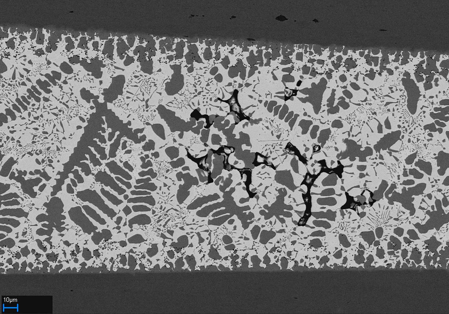
Metallographic investigations serve to describe the structure of materials qualitatively and quantitatively using microscopic methods. For metallographic analyses, cross-sections are prepared using advanced preparation procedures (such as mechanical, electrochemical, chemical). The microstructures are then examined on these cross sections using light microscopy or scanning electron microscopy and characteristics such as phase proportions, grain sizes, grain size distribution, particle sizes and precipitates are determined. This allows us to provide in-depth analysis of materials and enables high-quality failure and fracture analysis.
- Light microscopy
With the help of various modern light microscopes (stereo and reflected light microscopy), surface structures can be displayed in detail. These include, among other things, the analysis of fracture surfaces, metallographic examinations, measurement of layer thicknesses in cross sections, and much more.
- Electron Microscopy:
High-resolution imaging examinations of material samples and components are carried out using scanning electron microscopy (SEM). The use of different detectors provides different information about the structure of the surface being examined: the topography can best be imaged with secondary electrons (SE detector), while backscattered electrons (BSE detector) are used for material contrast images. An in-lens detector enables high-resolution images with resolutions down to the nm range.
Furthermore, the sample surface can be processed in-situ on a sub-µm scale using a focused ion beam (FIB) to examine the area immediately below the surface. This is used, for example, to analyse layer structures or in failure analysis. Imaging the sample using an ion beam also enables the grain structure to be displayed in high contrast.
The SEMs are also equipped with modern EDX systems to enable chemical analysis of the examined surface (or in the FIB section). More complex questions can be investigated using line scans, which show the concentration course for selected elements.
To examine the crystalline structure of a material in detail, electron backscatter diffraction (EBSD) is available. With this modern method, microstructures can be examined with high lateral resolution to determine the following characteristics: identification of individual phases, examination of grain boundaries, differences in orientation of neighbouring grains, identification of precipitates, etc.
- Surface Analysis based on 3D-models:
Surfaces are investigated using optical methods to determine the roughness, waviness and flatness of a surface. On the one hand, certain structures (e.g. peaks, valleys, grooves, pores, particle adhesions, etc.) can be measured and, on the other hand, the surface can be quantitatively characterized (determination of Ra, Rz and other statistical surface characteristics). The quantitative parameters are determined from 2D profile measurements and 3D surface measurements.
As an alternative to using purely optical methods, it is also possible to generate a digital surface model from SEM images using complex software programs and to derive the above-mentioned surface parameters from this model. This enables the assessment of waviness and roughness as well as the measurement of structures even on surfaces that are not accessible to optical inspection (e.g. miniature gearing of transmission parts).
- (Micro-) Hardness Testing:
You can find all information about (micro-) hardness testing here.
- Layer thickness measurement
Measuring the layer thickness is an essential component in the development of new layer systems and for analysing existing functional layers (e.g. in the frame of a damage analysis). The thickness of layer systems typically ranges from a few nanometres to a few micrometres. Depending on the type of coating, the substrate and the desired resolution, different methods are used: In a destructive test, the sample is cross-cut and the micrograph is examined using light- and electron microscopic methods. A minimally destructive method is measuring the layer thickness on an in-situ prepared FIB section: sample material is removed in a range of a few µm using a focused ion beam and the resulting cut surface is analysed. The area outside the FIB cut remains untouched.

